Understanding the W25Q256JVEIQ and Common Issues
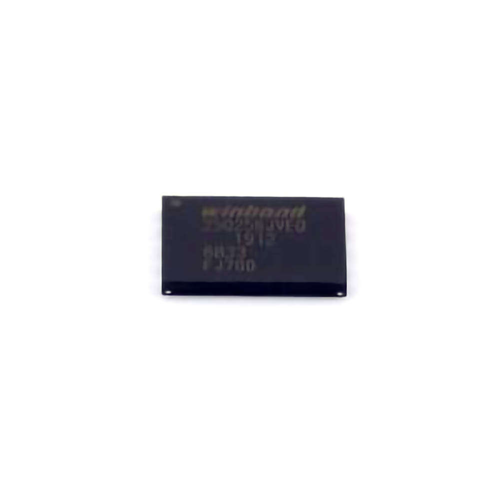
The W25Q256JVEIQ is a 256Mb (32MB) Serial NOR Flash memory chip from Winbond Electronics. It's widely used in embedded systems, networking equipment, consumer electronics, and automotive applications. With its high-speed SPI (Serial Peripheral interface ) interface and its advanced features, this chip is designed to meet the demands of modern devices. However, like any electronic component, it’s prone to certain operational issues that engineers and developers must address in order to ensure seamless performance.
1.1 Overview of the W25Q256JVEIQ
The W25Q256JVEIQ is a part of Winbond's W25Q series of NOR Flash memories, offering high-density storage with reliable data retention. It supports various read/write operations, such as sequential, random, and burst reads, as well as programmable erase and write capabilities. Its SPI interface is compatible with a wide range of microcontrollers and processors, making it a versatile choice for many applications.
Key Features:
256Mb (32MB) memory capacity
SPI clock speeds up to 133 MHz
Supports quad I/O (Quad SPI) for faster data transfer
Endurance of 100,000 program/erase cycles
Data retention of up to 20 years
Supports features like sector erase, block protection, and deep Power -down mode
Despite its high reliability and performance, users often encounter a few common issues during integration and usage. These problems can range from simple Communication failures to more complex Electrical or software malfunctions. This article explores these typical issues and offers solutions to resolve them.
1.2 Common Issues with W25Q256JVEIQ
1.2.1 Communication Failures (SPI Errors)
One of the most frequent problems developers face when using the W25Q256JVEIQ is communication failure via the SPI interface. This can manifest in different ways, including read/write operations not completing, the chip not responding, or data being corrupted. Here are some common causes and potential solutions:
Possible Causes:
Incorrect SPI clock settings: The chip may not communicate correctly if the clock polarity (CPOL) or clock phase (CPHA) settings are wrong. The W25Q256JVEIQ typically requires CPOL=0 and CPHA=0 for proper communication.
Incorrect chip select (CS) pin handling: If the Chip Select pin is not being asserted or deasserted properly, the device will not respond correctly. Make sure the CS pin is pulled low when initiating communication and returned high when the operation is completed.
Mismatched voltage levels: The chip operates at 3.3V logic levels, and interfacing with a 5V system can cause communication issues.
Solutions:
Double-check the SPI settings: Ensure the clock polarity and phase are configured correctly according to the datasheet. For standard SPI operations, CPOL=0 and CPHA=0 are typical, but consult the datasheet for specific configurations.
Verify CS pin functionality: Ensure that the CS pin is properly controlled by the microcontroller. The CS must be low at the start of each SPI transaction and returned high once the transaction is complete.
Check voltage levels: Ensure that the W25Q256JVEIQ is receiving the correct voltage levels (typically 3.3V). If you are using a 5V system, level shifting may be necessary.
1.2.2 Data Corruption and Unexpected Behavior
Data corruption can occur during read/write operations if the W25Q256JVEIQ experiences power interruptions, incorrect voltage levels, or issues with the internal memory management.
Possible Causes:
Power loss during write operations: If the chip experiences a sudden power loss during a write operation, it may cause incomplete data writes, leading to corruption.
Improper voltage levels: As mentioned earlier, improper voltage levels (e.g., 5V logic interfacing with a 3.3V chip) can lead to unreliable data storage and corruption.
Overwriting protected memory areas: If certain sectors or blocks are write-protected or locked, attempting to write to them can result in failed operations or corrupted data.
Solutions:
Ensure stable power supply: Implementing a power-fail detection circuit can help ensure that the chip completes its operations before power loss. Consider adding capacitor s or a battery-backed power system to prevent sudden power loss during writes.
Implement proper voltage level conversion: If using a 5V system, ensure that the voltage levels are shifted correctly to match the 3.3V logic of the W25Q256JVEIQ.
Manage write protection: Always check that the memory areas you intend to write to are not write-protected. Review the chip’s status register to ensure no write protection bits are set in critical areas.
1.2.3 Programming Failures (Erase/Write Failures)
When attempting to program or erase data on the W25Q256JVEIQ, you may encounter failures or incomplete operations. This can be caused by various factors, including Timing issues, incorrect command sequences, or hardware faults.
Possible Causes:
Timing issues: The W25Q256JVEIQ has specific timing requirements for its write and erase operations. If these timing parameters (such as the chip select pulse width or delay times) are violated, the operation may fail.
Incorrect command sequence: Each erase or write operation requires specific commands. For example, before erasing a sector, you need to send the correct unlock command. Failure to follow the correct sequence can result in operation failure.
Chip being in a deep power-down mode: The W25Q256JVEIQ can enter a deep power-down mode to conserve energy. In this state, the chip is unresponsive to read or write commands.
Solutions:
Adhere to timing specifications: Carefully review the timing diagrams in the datasheet and ensure that your code respects all timing constraints. This includes the necessary delay between commands and chip-select signal handling.
Follow the correct command sequence: Ensure that you’re sending the correct sequence of commands. For example, to erase a sector, you first need to send an unlock command followed by the erase command. Check the datasheet for detailed command sequences.
Exit deep power-down mode: If the chip is in deep power-down mode, send the appropriate wake-up command to bring the chip back to an active state before attempting any further operations.
Advanced Troubleshooting and Tips for Optimizing Performance
While the issues discussed in Part 1 cover some of the more common challenges with the W25Q256JVEIQ, there are several advanced troubleshooting techniques and tips that can help you optimize performance, avoid errors, and improve the overall reliability of the system.
2.1 Advanced Electrical Troubleshooting
2.1.1 Power Supply Noise and Stability
Power supply noise or instability can have a significant impact on the operation of flash memory. The W25Q256JVEIQ is highly sensitive to voltage fluctuations, and noise can result in data corruption, erratic behavior, or communication failures.
Solution:
Use low-dropout (LDO) regulators and decoupling capacitors close to the chip to filter out noise and stabilize the power supply. A combination of 0.1µF and 10µF ceramic capacitors can be effective in reducing high-frequency noise.
2.1.2 Signal Integrity and Trace Lengths
Long SPI traces or poor signal integrity can introduce communication errors, especially when high-speed operations are used (e.g., Quad SPI mode). Signal degradation can lead to miscommunications or failed operations.
Solution:
Minimize trace lengths between the microcontroller and the W25Q256JVEIQ. If possible, use controlled impedance traces to maintain signal integrity.
Use pull-up/pull-down resistors on SPI lines to ensure that they are in the correct state when not actively driven.
2.1.3 Static Electricity and ESD Protection
Flash memory chips like the W25Q256JVEIQ are sensitive to electrostatic discharge (ESD), which can permanently damage the internal circuits or cause intermittent failures.
Solution:
Implement ESD protection diodes or use ESD mats and grounding straps when handling the chip during development and testing. Proper PCB grounding and shielding can also help minimize the risk of ESD-related failures.
2.2 Software and Firmware Considerations
2.2.1 Data Integrity Checks
In embedded systems, ensuring data integrity is critical. The W25Q256JVEIQ supports several features like write verification and status register checking, but these require careful software handling.
Solution:
Implement data verification after each write operation. This ensures that data written to the chip is correctly stored and can be read back without errors. Consider using checksums or error-detecting codes to ensure the integrity of larger data blocks.
2.2.2 Optimizing Write Operations
Flash memory has a finite number of write/erase cycles, and overuse can cause premature wear. Developers must consider wear leveling and write optimization when using the W25Q256JVEIQ.
Solution:
Implement wear leveling algorithms to distribute write operations evenly across the chip’s memory sectors. This prevents certain areas of the chip from wearing out prematurely.
Use block-level writes rather than small byte writes to minimize the number of write cycles and maximize memory lifespan.
2.2.3 Handling Power Loss Scenarios
A sudden power failure during write or erase operations can cause data corruption or incomplete writes. In critical applications, handling these situations with a robust fail-safe mechanism is crucial.
Solution:
Implement a power-fail detection circuit that allows you to monitor the power supply and initiate a safe shutdown procedure or store critical data to a backup area in case of power loss.
2.3 Additional Tips for Maximizing Performance
Leverage Quad SPI Mode: The W25Q256JVEIQ supports Quad SPI, which allows for faster data transfers. If your system supports it, enable Quad SPI mode for higher throughput, especially when dealing with large data blocks.
Use Block Protection: For sensitive or critical areas of memory, use the chip’s block protection features to prevent accidental overwrites.
Conclusion
The W25Q256JVEIQ is a robust and versatile flash memory solution, but like any complex component, it requires attention to detail during integration and use. By understanding common issues and following best practices for both hardware and software, you can significantly reduce troubleshooting time and enhance the reliability of your embedded systems. Whether you're facing SPI communication failures, data corruption, or programming issues, the solutions provided here offer a comprehensive guide to diagnosing and resolving these challenges efficiently. With the right approach, your system can achieve optimal performance and long-lasting reliability.
Partnering with an electronic components supplier sets your team up for success, ensuring the design, production, and procurement processes are quality and error-free.

