Understanding the ADS1114 Low- Power ADC
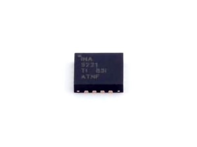
The ADS1114 is a 16-bit Analog-to-Digital Converter (ADC) from Texas Instruments, widely used in applications where high precision, low power consumption, and small form factor are paramount. This ADC is particularly popular in battery-operated and portable devices, where conserving power while maintaining measurement accuracy is crucial.
1.1. Key Features of ADS1114
At the core of its appeal, the ADS1114 provides excellent accuracy and resolution, capable of converting analog signals to digital data with a resolution of 16 bits. It operates on a supply voltage of 2.0V to 5.5V, which allows flexibility for use in a range of systems from low-voltage portable devices to higher-voltage industrial equipment.
The ADS1114 offers a programmable gain amplifier (PGA) that can scale the input signal. This feature ensures that the ADC can measure signals across a wide range of magnitudes. The PGA allows for input voltages from ±256 mV to ±6.144V, depending on the chosen gain setting. Furthermore, the ADS1114 supports I2C Communication , making it easy to interface with microcontrollers and other embedded systems.
One of the standout features of the ADS1114 is its low power consumption. In many applications, power efficiency is a critical factor, and the ADS1114 excels with a typical current consumption of only 150 µA in its continuous conversion mode. This makes it ideal for battery-operated systems, where maintaining long battery life is essential. Additionally, it features an ultra-low power shutdown mode, drawing only 1.5 µA when idle, which helps to further extend the operational life of the system.
1.2. Applications of ADS1114
The versatility of the ADS1114 makes it suitable for a wide range of applications. It is especially beneficial in precision Sensor interfacing, such as:
Temperature Sensors : When paired with temperature sensors such as thermistors or RTDs (resistance temperature detectors), the ADS1114 provides high-accuracy temperature measurements. The wide input voltage range and precision allow for fine-grained temperature readings in industrial, automotive, and environmental monitoring systems.
Strain Gauges: The ADS1114’s programmable gain amplifier is ideal for amplifying low-level signals from strain gauges in applications such as load cells and structural health monitoring.
Medical Devices: In medical instruments such as ECG or EEG systems, the ADS1114 can capture minute analog signals, converting them with high accuracy to digital form for analysis.
Portable Instruments: Due to its low power requirements, it is highly suitable for handheld and battery-powered devices that demand high-precision data acquisition.
1.3. Data Conversion Process
The data conversion process in the ADS1114 follows the standard principles of an ADC, but its precision and functionality offer a deeper understanding. The conversion process involves the following steps:
Input Signal Sampling: The first step in the process is the sampling of the input analog signal. This is achieved through a sample-and-hold circuit that temporarily holds the signal voltage constant for the conversion process.
Analog-to-Digital Conversion: The ADS1114 converts the analog voltage into a digital output through a successive approximation register (SAR). The SAR ADC algorithm iteratively compares the input signal to a reference voltage and approximates the value using a binary code.
Output Digital Code: The 16-bit output from the conversion process provides a digital representation of the analog input voltage. This output can then be sent to a microcontroller or other processing units for further analysis.
1.4. Noise Reduction and Accuracy Enhancement
High-precision ADCs like the ADS1114 often deal with noise, which can degrade the accuracy of the measurements. Noise in ADCs can originate from several sources, including power supply fluctuations, electromagnetic interference ( EMI ), and even thermal noise within the system components.
To mitigate this, the ADS1114 features integrated features such as a programmable input filter to reduce noise from the signal source. Additionally, it uses a well-designed internal reference voltage (typically 2.048V or 4.096V) to ensure consistent and stable measurements across varying conditions.
Furthermore, to reduce the impact of noise during the sampling phase, the ADC’s sampling rate can be configured, balancing between measurement speed and noise rejection. Slower sampling rates often lead to better noise rejection but at the cost of slower data acquisition.
Designing a High-Precision Sampling Circuit with the ADS1114
While the ADS1114 is an excellent ADC on its own, achieving high-precision results requires careful attention to the surrounding circuit design. This section discusses how to design a high-precision sampling circuit that takes full advantage of the ADS1114’s capabilities.
2.1. Power Supply Considerations
One of the primary factors affecting the accuracy of an ADC like the ADS1114 is the quality of the power supply. Fluctuations in the supply voltage can introduce noise into the ADC, which will degrade the precision of the digital output. Therefore, it is critical to ensure that the ADC receives a stable and clean power supply.
Low-Noise Power Regulators: Using low-noise voltage regulators is highly recommended when powering the ADS1114. Linear regulators, such as the LP5907, provide stable, clean power to sensitive analog components like ADCs.
Decoupling Capacitors : Proper decoupling capacitor s should be placed close to the ADS1114’s power pins to reduce high-frequency noise. Typically, a combination of a 0.1µF ceramic capacitor and a 10µF electrolytic capacitor is used to filter out both high- and low-frequency noise.
2.2. Signal Conditioning and Amplification
Before the analog signal is fed into the ADS1114, it often requires some form of conditioning. This could include amplification, filtering, or level shifting. Given the programmable gain amplifier (PGA) in the ADS1114, the incoming signal should be optimized to use the full dynamic range of the ADC without causing clipping or excessive noise.
Gain Selection: The PGA of the ADS1114 allows for several gain settings, ranging from 1 to 16. For signals that are too weak, increasing the gain can boost the signal level before conversion. However, too high of a gain can saturate the input range, so it’s essential to choose the appropriate gain setting for the expected signal amplitude.
Buffering the Input Signal: In some cases, especially when interfacing with high-impedance sources like sensors, the input signal may require buffering to prevent loading effects. A low-offset operational amplifier can be used as a buffer to provide a high-impedance input to the ADS1114.
2.3. Noise Reduction and Filtering Techniques
As mentioned earlier, noise is a significant concern in high-precision ADC applications. To reduce the impact of noise on the measurement, several techniques can be applied.
Low-Pass Filters: A low-pass filter can be implemented at the input stage to reduce high-frequency noise components. A simple RC (resistor-capacitor) filter can help smooth out high-frequency spikes that might otherwise be sampled by the ADC.
Shielding and Grounding: Proper shielding of the analog front-end and grounding techniques can also significantly reduce electromagnetic interference (EMI) that might affect the ADC’s operation. Ground planes should be used to minimize noise coupling, and careful routing of analog signals away from digital lines helps maintain signal integrity.
2.4. Optimal Sampling Rate Configuration
The ADS1114 offers flexible sampling rates, ranging from 8 to 860 samples per second (SPS). The sampling rate must be chosen based on the nature of the input signal and the tradeoff between accuracy and speed. For example, slow-varying signals might benefit from slower sampling rates, which can offer better resolution and noise rejection.
Slower Sampling for Noise Rejection: Slower sampling rates (e.g., 8 SPS) are preferable for applications requiring higher accuracy and noise immunity, as they allow more time for the ADC to settle and average out noise.
Higher Sampling for Faster Updates: In cases where faster data acquisition is necessary (e.g., for high-speed dynamic signals), higher sampling rates (e.g., 860 SPS) can be used, though they may come at the cost of lower resolution and increased noise sensitivity.
2.5. I2C Communication and Data Processing
Once the ADC has converted the analog signal to a digital output, it communicates the data through I2C, a widely-used protocol in embedded systems. The I2C interface is simple to implement and allows for easy communication between the ADS1114 and a microcontroller or processor.
Data Handling: The digital data from the ADC can be processed by a microcontroller to extract meaningful information, perform calculations, or send the data to a display or storage unit. Proper software handling of the I2C interface, including error checking and data validation, ensures the system runs reliably.
Conclusion
The ADS1114 is a remarkable low-power, high-precision ADC that offers a wide range of capabilities for embedded and battery-powered applications. By understanding its key features, such as its high-resolution conversion, programmable gain amplifier, and I2C interface, and by carefully designing a supporting circuit that addresses power supply stability, signal conditioning, and noise reduction, engineers can achieve optimal performance for a variety of applications. Whether you're working with sensors in medical devices, industrial equipment, or portable instruments, the ADS1114 can help you achieve accurate, reliable measurements while maintaining power efficiency.
If you are looking for more information on commonly used Electronic Components Models or about Electronic Components Product Catalog datasheets, compile all purchasing and CAD information into one place.


