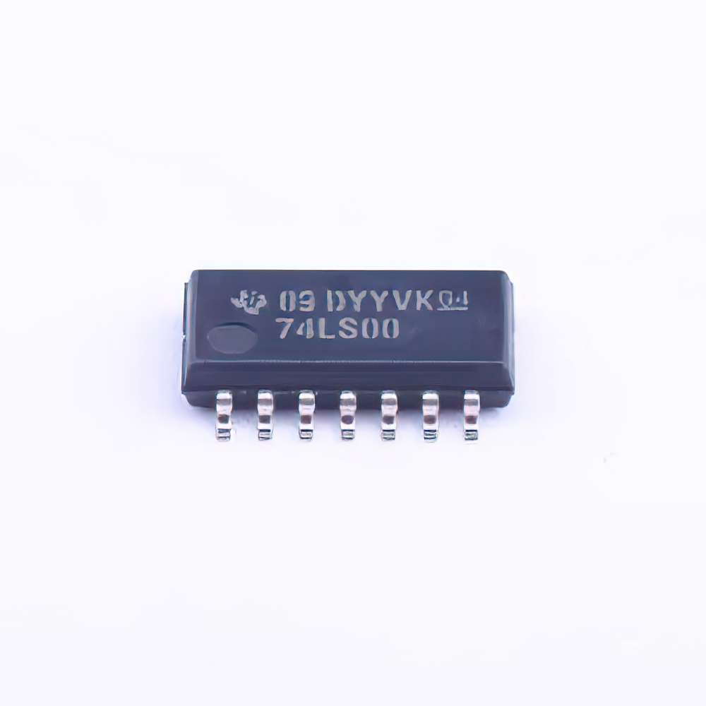
Introduction to SN74LS00 and Basic Logic Gates
In the world of digital electronics, logic gates are fundamental building blocks used to perform Boolean algebra operations. These gates are available in various forms, and the SN74LS00 IC is one of the most widely used components for implementing logic gate functions. In this article, we will explore the SN74LS00, its characteristics, and how logic gate circuits, based on this IC, form the backbone of modern electronic devices.
Understanding the SN74LS00 IC
The SN74LS00 is a part of the Texas Instruments’ LS (Low Power Schottky) series of integrated circuits (ICs). It is a quad 2-input NAND gate IC, which means it contains four independent 2-input NAND gates within a single package. The primary function of these gates is to perform the NAND operation, which is one of the fundamental operations in digital logic.
A NAND gate (NOT AND) is a digital logic gate that outputs a low signal (0) only when both of its inputs are high (1); otherwise, it outputs a high signal (1). In Boolean algebra, this operation is represented as:
[
A \cdot B = \overline{A \cdot B}
]
where A and B are the inputs, and the overline indicates the NOT operation.
The SN74LS00 IC is widely used because it offers high-speed logic operations with low power consumption, making it ideal for a variety of digital applications such as combinational and sequential logic circuits.
Characteristics of the SN74LS00 IC
Before diving deeper into practical applications, it is essential to understand the key characteristics of the SN74LS00 IC:
Package Type: Typically available in 14-pin Dual In-Line Package (DIP) or Surface Mount (SMT) packages.
Voltage Range: It operates with a voltage supply of 4.5V to 5.5V, making it compatible with most TTL (Transistor-Transistor Logic) systems.
Speed: The IC is designed for high-speed performance, with a propagation delay time (tpd) of approximately 20ns at Vcc = 5V.
Power Consumption: Due to its Schottky technology, the SN74LS00 consumes less power compared to traditional TTL circuits, improving overall system efficiency.
Temperature Range: It is suitable for use in most standard temperature conditions, typically from 0°C to 70°C.
The combination of these characteristics makes the SN74LS00 an ideal choice for many applications in digital electronics.
Basic Logic Gate Functions
To fully appreciate the capabilities of the SN74LS00 IC, it’s important to understand the basic types of logic gates it uses. These are:
AND Gate: An AND gate outputs a high signal (1) only when both inputs are high (1). In Boolean terms, ( A \cdot B ).
OR Gate: An OR gate outputs a high signal (1) when at least one input is high (1). It is represented as ( A + B ).
NOT Gate: A NOT gate inverts the input signal. If the input is 1, the output is 0, and vice versa.
NAND Gate: A NAND gate is simply an AND gate followed by a NOT gate. Its output is low (0) only when both inputs are high (1). It is represented as ( \overline{A \cdot B} ).
NOR Gate: A NOR gate is an OR gate followed by a NOT gate. It outputs high (1) only when both inputs are low (0).
XOR Gate: An XOR gate (Exclusive OR) outputs high (1) only when the inputs are different (i.e., one is high and the other is low).
XNOR Gate: The XNOR gate is the complement of the XOR gate. It outputs high (1) when both inputs are the same.
Among these, the NAND gate is particularly important because it is considered a universal gate. This means that any other logic gate can be implemented using just NAND gates.
The SN74LS00 IC is specifically designed to provide a high-speed, reliable implementation of the NAND gate, making it an essential component for creating complex digital circuits.
Using SN74LS00 to Build Logic Circuits
Let’s consider a few simple logic circuits built using the SN74LS00 NAND gates. Understanding these examples will give you insight into how this IC fits into real-world digital systems.
Example 1: Simple NAND Gate Logic
Suppose we want to implement a simple NAND gate logic circuit with two inputs (A and B). The output will be high (1) unless both inputs are high (1), in which case the output will be low (0).
Input A and B are fed into the two inputs of one of the NAND gates in the SN74LS00 IC.
The output of the NAND gate will be the result of the operation ( \overline{A \cdot B} ).
This simple circuit is an excellent starting point for understanding how digital systems perform logic operations using the SN74LS00 IC.
Example 2: Implementing an Inverter (NOT Gate) with NAND Gates
Interestingly, you can create a NOT gate (inverter) by connecting both inputs of a NAND gate to the same signal. In Boolean terms, if both inputs are A, the NAND operation will produce:
[
\overline{A \cdot A} = \overline{A}
]
This demonstrates how a NAND gate can be used to simulate the behavior of a NOT gate.
Example 3: Implementing a Half Adder Circuit
A half adder is a fundamental circuit that adds two binary digits. It outputs a sum and a carry. To implement this using only NAND gates, we need to combine multiple NAND gates.
Sum: The sum output of a half adder is the XOR of the two inputs.
Carry: The carry output is the AND of the two inputs.
By using the SN74LS00 IC, you can combine multiple NAND gates to realize the XOR and AND operations needed to create the full half adder.
In this way, the SN74LS00 IC helps us implement basic arithmetic functions that are at the core of digital systems.
Advanced Applications and Design Considerations of SN74LS00 in Logic Gate Circuits
As we’ve seen, the SN74LS00 IC provides a flexible and efficient way to implement basic logic gates. Now, let’s delve into more advanced applications and design considerations where the SN74LS00 and similar TTL ICs play a significant role in digital electronics.
Advanced Applications of SN74LS00 in Digital Systems
The SN74LS00 IC is more than just a tool for creating basic logic gates. Its versatility allows it to be used in more complex circuits that are essential for various electronic applications.
Example 1: Creating Complex Digital Systems
Digital systems, such as microprocessors, controllers, and digital signal processors, rely on a combination of logic gates to perform operations. While the SN74LS00 is not typically used in the processing core of these systems, it plays an essential role in creating the fundamental components.
For example, you can use the SN74LS00 IC to build flip-flops, counters, multiplexers, and more complex sequential circuits. These components form the foundation of control systems in microcontrollers, allowing them to store and manipulate data.
Example 2: Building a Digital Clock
A digital clock is a practical example of a system that utilizes logic gates for its operation. The SN74LS00 IC can be used to design the circuit that handles timekeeping and displays the output on a digital display.
In a digital clock, counters are used to keep track of seconds, minutes, and hours. These counters are implemented using flip-flops, which in turn are built from logic gates like those in the SN74LS00. The outputs from these flip-flops are then used to drive a 7-segment display or other types of digital displays to show the time.
Example 3: Error Detection and Correction Circuits
In communication systems, data is often transmitted over long distances, where errors may occur due to noise or other factors. Logic circuits built from SN74LS00 NAND gates can be used to detect and correct errors in data transmission.
Parity check circuits, cyclic redundancy checks (CRC), and other error detection schemes rely on logical operations that can be implemented with the SN74LS00. For example, a parity bit, which is used to check whether a binary number has an even or odd number of 1s, can be generated using NAND gates to ensure data integrity.
Example 4: Memory Circuit Design
Memory devices, such as RAM and ROM, rely on complex circuits that can store and retrieve data. The SN74LS00 IC can be used in the design of certain types of memory cells, especially in simpler applications where small amounts of data need to be stored.
For instance, a static memory cell, which retains its data as long as power is supplied, can be implemented using flip-flops or latches that are built with NAND gates.
Design Considerations and Challenges
When designing logic circuits using the SN74LS00 IC, there are several important design considerations and challenges to keep in mind.
1. Timing and Propagation Delay
Each logic gate introduces a small delay between the input and the output, known as propagation delay. While the SN74LS00 IC is designed for high-speed operations, in large, complex circuits, these delays can accumulate, leading to timing issues.
To mitigate this, designers often optimize circuit layouts and choose components with low propagation delays. For highly time-sensitive applications, such as high-speed data processing, the selection of ICs with minimal delay is critical.
2. Power Consumption
While the LS series ICs, including the SN74LS00, are designed for low power consumption compared to traditional TTL devices, it is still important to consider the overall power budget of the circuit. In portable devices, power efficiency is crucial, so designers may choose alternative logic families, such as CMOS (Complementary Metal-Oxide-Semiconductor), which typically offer even lower power consumption than LS series TTL ICs.
3. Noise Immunity
TTL circuits like the SN74LS00 are sensitive to noise, which can cause logic errors or instability. Ensuring proper grounding, decoupling capacitor s, and using shielded cables are important steps in preventing interference and ensuring reliable operation in noisy environments.
Conclusion
The SN74LS00 IC is a cornerstone in the field of digital electronics. With its four independent 2-input NAND gates, it enables designers to create a wide variety of logic circuits for applications ranging from simple digital systems to complex memory and control systems. Understanding the SN74LS00 and how it fits into the larger world of digital logic design is crucial for anyone interested in the field of electronics.
As digital systems continue to evolve and grow in complexity, the basic principles of logic gates and their efficient implementation, such as through the use of the SN74LS00, will remain integral to the development of future technologies. Whether you are designing a simple circuit or working on cutting-edge electronics, mastering the basics of logic gates is the first step toward becoming an expert in the exciting world of digital design.
Partnering with an electronic components supplier sets your team up for success, ensuring the design, production, and procurement processes are quality and error-free.


